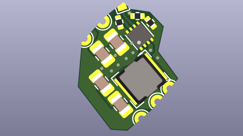
Some time ago, while designing the PCB for the Sony Vaio replacement motherboard, I went on a quest to find a perfect 5 V boost regulator. Requirements are simple – output 5 V at about 2A , with input ranging from 3 V to 5 V, and when the input is 5 V, go into “100% duty” (“pass-through”/”bypass”) mode where the output is directly powered from the input, saving me from any conversion inefficiencies for USB port power when a charger is connected. Plus, a single EN pin, no digital configuration, small footprint, no BGA, no unsolicited services or offers – what more could one ask for.
As usual, I go to an online shop, set the parameters: single channel, all topologies that say “boost” in the name, output range, sort by price, download datasheets one by one and see what kind of nice chips I can find. Eventually, I found the holy grail chip for me, the MIC2876, originally from Micrel, now made by Microchip.
MIC2876 is a 5 V regulator with the exact features I describe above – to a T! It also comes with cool features, like a PG “Power good” output, bidirectional load disconnect (voltage applied to output won’t leak into input), EMI reduction and efficiency modes, and it’s decently cheap. I put it on the Sony Vaio board among five other regulators, ordered the board, assembled it, powered it up, and applied a positive logic level onto the regulator’s EN pin.
Immediately, I saw the regulator producing 3 V output accompanied by loud buzzing noise – as opposed to producing 5 V output without any audible noise. Here’s how the regulator ended up failing, how exactly I screwed up the design, and how I’m creating a mod board to fix it – so that the boards I meticulously assembled, don’t go to waste.
Some Background… Noise
This regulator is one angry chip – with a 2 MHz switching speed, it’s relatively high as far as regulators go. More common is to see 1 MHz and below. Higher switching speed means it can use a smaller inductor, which is great for routability. It also might not handle some layout or component mistakes that a lower-frequency regulator might do.
Still, I made a number of good choices. With boost regulators, remember – you have to pick an inductor according to the input current, not output current; recalculate accordingly, and check the efficiency graphs. That, I achieved – while I was limited by the size of the inductor I could fit onto the board, I did find a 3.8 A inductor that let me achieve a little under 2 A output. Iin theory – good enough. All places where 5 V could go on the board are current-limited, and there are just two USB ports I need to power, so even 1.5 A of 5 V output is plenty. I also picked proper footprints for both inductors and capacitors – it can be tricky to find 22 uF 10 V capacitors in 0603, but it’s a breeze if you pick 0805. A regulator can fail if you don’t provide it with the kind of capacitance that the datasheet asks for, but I put two footprints on both input and output, and it let me experiment with output caps.


On the other hand, you might have already noticed at least one problem if you’ve read the layout article thoroughly. For one, see that feedback divider? It’s supposed to be connected after the capacitors, measuring the output – not directly between the inductor and the capacitors, which is a point where a lot of current flows back and forth. I’m not sure how I didn’t catch myself doing this, given that I thoroughly described in an article in the same timeframe that I was routing this board; it’s the kind of mistake you can’t help but write off to general human fallibility. There are a good few problems, though – I should have reconsidered this layout severely before ordering.
Example Layout As Checklist Item
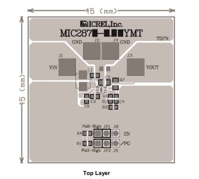
A contributing factor, I’m sure, is that the datasheet doesn’t have a layout example – you only have the evaluation board documentation to go off of, and I didn’t get that far. It’s not always that the datasheet recommendation will be reasonable, or look reasonable. For instance, in the last article, where I reviewed switching regulator layouts, I’ve shown the TI’s puzzling proposed layout for a buck regulator chip of theirs – with intentions hard to decypher both for me and for fellow hackers in the comment section.
However, it helps way more often than it might puzzle you, and if you never even see the layout example because you have to hunt down extra documents for it, you might not notice fundamental differences, just like I did not notice them. The bottom line is I should have noticed the missing layout example and hunted down the evaluation board datasheet.
Comparing mine with the example layout, you might notice another problem. My ground routing differs a fair bit, and it sure seems that my routing is inferior – my ground is more isolated islands, with a fair bit of ground return current forced to go through vias, and the example layout has a fairly straightforward ground path, no underside layers strictly required. What’s more – you might notice ground return current flowing between output capacitors and the regulator center pad, which will go by the pin 4 – AGND. AGND is specifically a pin supposed to stay away from the switching loop pins, and I do remember noticing this at some point, thinking I should revisit the layout and see if I have fulfilled this obligation. It stayed as a low-level mental TODO in my brain, one that I never actually revisited.
One last thing is placing components under the regulator. I can’t quite afford to free up the under-regulator space on the opposite layer of the board – the board is tightly packed by necessity. My defense is that this is a 4-layer board, with two inner layers dedicated to ground, but I’m not sure whether that negates the concerns of the engineers who wrote this recommendation. This is the only thing I’m leaving in when it comes to v2 board design – otherwise, let’s take a look!

Out of interest and wanting to finally get to the bringup, I re-wired the FB connection using magnet wire, and even added a more direct GND connection for the output capacitors along the way. The regulator’s behaviour didn’t change one bit, however. Either the GND layout is seriously critical (likely), or the chip got damaged after being booted up with a miswired feedback network; whichever option it is, looks like things won’t be as quick as that. In general, I spent four-five hours on this particular issue, slowly realizing that it’s screwed up beyond fixing.
No matter – let’s just design a mod board that works around all of my mistakes. This helps me bring up the v1 PCB fully – wouldn’t want to have $300 worth of components and days of assembly going to waste. Also, after just a few modifications, we will have a cool switching regulator breakout that we can all use as a building block!
Quick, Simple, Powerful
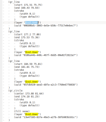
To make a modification like this, I start by marking an outline of the mod on one of the User layers, then open the file in a text editor, Ctrl-F for the User layer name I used, copy all the lines and circles – and paste them into a footprint .kicad_mod file that’s also open in a text editor. There are a few caveats – first one, the User.Eco2 layer in KiCad UI is called Eco2.User in the actual file. Then, as you copy-paste graphics you’ve drawn, you will also want to replace all “gr_” with “fp_”. Remember to close your kicad_mod while pasting contents into it in the text editor – otherwise, it can be overwritten by accident. Finally, open your .kicad_mod in the footprint viewer, box-select your new lines, and move them so that the (0,0) center point is somewhere near the outline, because it’s going to be a bother to handle this footprint otherwise.



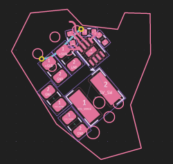

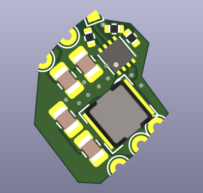 Then, open a new PCB project, copy-paste the 5 V boost schematic block into the schematic, open the footprint association view and bring over any footprints missing, sync the PCB file, then duplicate the evaluation board layout. Thanks to this workflow, I quickly created a 5 V boost mod board I can solder on top of the board I currently have. This board is about to be ordered, with proper layout, and I’ll soon be soldering it onto the motherboard then testing it – expect an update in the comment section.
There are five (or, four and a half) other switching regulators on the same board, and, as I’m bringing them up and testing them, I’ll write one more article where I will be sharing lessons, whatever they turn out, showing you examples of how to pick parts for a switching regulator, plus, most certainly, demonstrating a couple more more little ways you might get things wrong and how to avoid them. So, till next time!